 跳到内容
跳到内容 
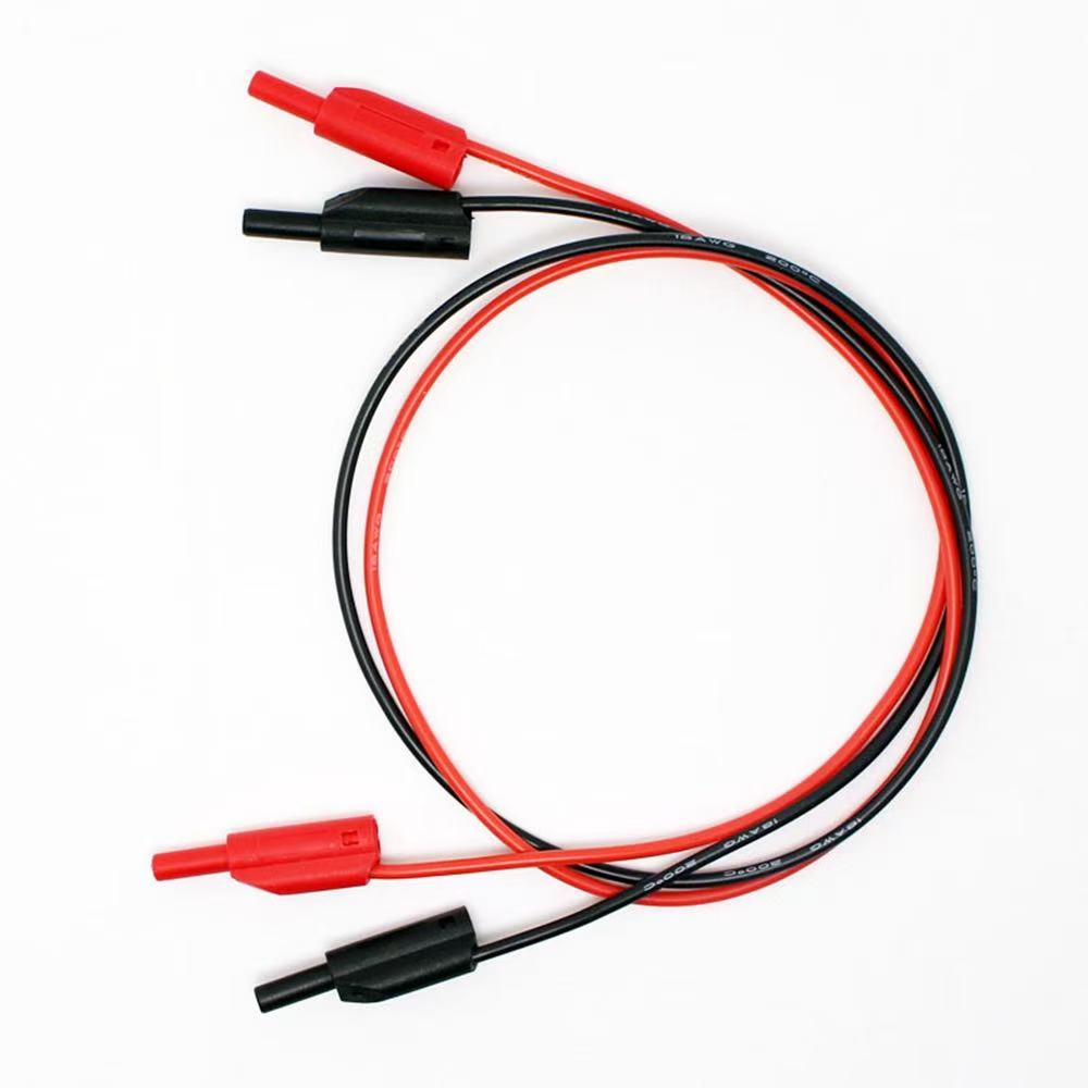
Table of Contents
In semiconductor manufacturing and quality assurance, the difference between a reliable product and a costly failure often comes down to test accuracy. While sophisticated test equipment receives most of the attention, experienced engineers know that seemingly mundane factors—from the condition of your test leads to the setup of your ESD workbench—can dramatically impact measurement precision. This comprehensive guide explores the critical yet often overlooked elements that separate accurate test results from misleading data.
The Hidden Variables Affecting Test Accuracy
Test accuracy in semiconductor environments doesn’t exist in a vacuum. Every measurement represents a complex interaction between the device under test (DUT), the measurement instrument, the connection pathway, and the surrounding environment. Understanding and controlling these variables separates competent testing from truly reliable characterization.
Understanding Measurement Chain Degradation
Before diving into specific control methods, it’s essential to recognize that your measurement is only as accurate as your weakest link. A million-dollar parameter analyzer means nothing if your connection path introduces noise, resistance variations, or intermittent contacts. This principle drives every accuracy control measure discussed in this article.
Test Leads: The Critical Connection You’re Probably Overlooking
Precision Test leads function as the nervous system of your measurement setup, yet they’re frequently treated as afterthoughts. This oversight can introduce errors ranging from subtle DC offsets to complete signal integrity collapse.
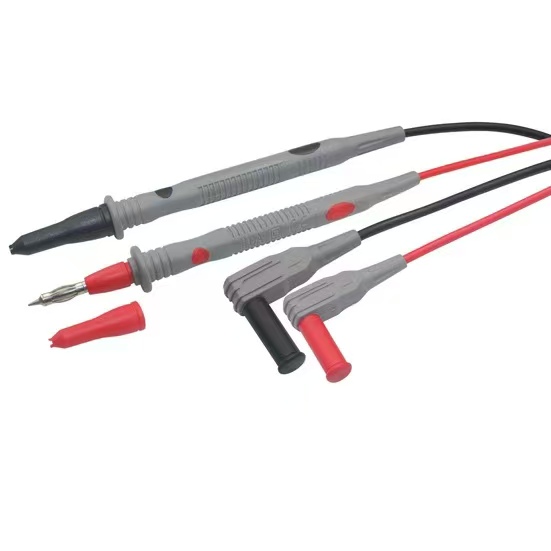
Contact Resistance: The Silent Accuracy Killer
One of the most insidious problems with test leads involves contact resistance at the probe tip. Over time, oxidation, contamination, and mechanical wear create resistive barriers that vary unpredictably. For low-current measurements or precision voltage testing, even a few hundred milliohms can skew results significantly.
Control strategy: Implement a regular probe inspection and cleaning schedule. For critical measurements, use four-wire (Kelvin) sensing configurations that eliminate lead resistance from the measurement path. This technique employs separate current-carrying and voltage-sensing leads, allowing the instrument to compensate for connection resistance automatically.
Capacitive and Inductive Loading
Test leads aren’t just resistive elements—they possess parasitic capacitance and inductance that increase with length. These parasitics create frequency-dependent impedances that distort high-speed signals and introduce phase shifts in AC measurements.
Control strategy: Minimize lead length whenever possible. For high-frequency measurements above 10 MHz, use coaxial cables with proper impedance matching (typically 50Ω). Position leads to minimize loop areas, reducing inductive pickup. Consider using active probes for sensitive measurements, as these present high input impedance while driving low-impedance outputs.
Mechanical Stability and Repeatability
Vibration, tension, and flexing of test leads can create triboelectric noise—where mechanical stress generates electrical signals. This phenomenon becomes particularly problematic in low-level current measurements (femtoamp to picoamp ranges) common in leakage testing.
Control strategy: Secure test leads using proper fixturing to prevent movement during measurement. Use low-noise cables specifically designed for sensitive applications—these feature conductive layers that drain triboelectric charges to ground. Allow adequate warm-up time after any cable movement, as trapped charges require minutes to dissipate.
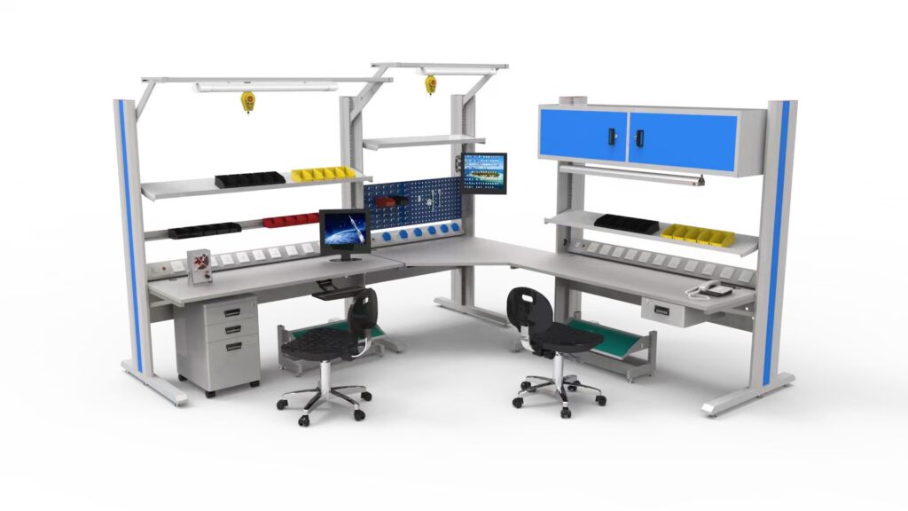
The ESD Workbench: Your Foundation for Reliable Testing
An ESD workbench does far more than prevent electrostatic discharge damage—it establishes the electrical environment where accurate measurements become possible. A properly configured ESD workstation creates a controlled reference plane and manages stray currents that would otherwise corrupt test data.
Establishing a Proper Ground Reference
Many accuracy problems stem from ground loops and undefined reference potentials. Your ESD workbench provides the physical platform for creating a single-point ground system where all equipment references a common potential.
Control strategy: Connect your ESD mat to a verified earth ground using the proper grounding point in your facility. Ensure all test equipment, the DUT fixture, and anti-static accessories bond to this same reference. Use a ground integrity monitor to continuously verify the connection resistance remains below 1 megohm. This unified ground plane prevents circulating currents and establishes a stable voltage reference for your measurements.
Managing the Electrostatic Environment
Electrostatic fields affect semiconductor testing in two distinct ways: catastrophic damage through ESD events and subtle measurement errors from field coupling. While the first receives ample attention, the second often goes unrecognized.
Control strategy: Maintain relative humidity between 30-50% to naturally dissipate static charges. This range prevents both excessive static buildup and condensation issues. Use ionizing air blowers to neutralize charges on insulators that cannot be grounded directly. Position the ionizer to create a balanced ion environment over your test area without creating air currents that disturb sensitive measurements.
Workbench Surface Conductivity Optimization
The conductive surface of your ESD workbench serves multiple functions: ESD protection, static dissipation, and electromagnetic shielding. However, improper surface resistance can actually introduce measurement errors.
Control strategy: Select ESD mat materials with surface resistance in the 10^6 to 10^9 ohm range. This range dissipates static safely while preventing excessive leakage currents that could reach your DUT. Avoid materials below 10^6 ohms for precision testing, as they can shunt small measurement currents. Regularly verify surface resistance using a calibrated surface resistivity meter, as aging and contamination degrade performance over time.
Temperature Control: The Variable Everyone Measures, Few Control Properly
Semiconductor characteristics exhibit strong temperature dependence, with some parameters changing several percent per degree Celsius. Yet temperature control often receives inadequate attention in test environments.
Thermal Gradients in the Test Setup
Even when ambient temperature is controlled, thermal gradients within your test fixture can create measurement drift. Power dissipation in the DUT, heating from nearby equipment, and airflow patterns all contribute to localized temperature variations.
Control strategy: Use thermal insulation or enclosures around your DUT fixture to minimize air current effects. For temperature-sensitive measurements, allow extended thermal soak time—often 10-15 minutes—before initiating testing. Monitor DUT temperature directly using thermocouples or RTDs placed as close to the active area as possible, rather than relying on ambient measurements.
Thermoelectric Effects in Connections
When dissimilar metals contact at different temperatures, they generate thermoelectric voltages (Seebeck effect). These voltages, though typically microvolts to millivolts, can dominate measurements of low-voltage semiconductor parameters.
Control strategy: Use contacts made from identical materials throughout the measurement path. Copper-to-copper connections minimize thermoelectric EMF. For ultra-precision DC measurements, place connection points in close thermal proximity or use thermal equalization blocks. If possible, reverse measurement polarity and average results to cancel thermoelectric offsets.
Electromagnetic Interference Mitigation
High-frequency switching power supplies, digital electronics, and RF communication devices create electromagnetic fields that couple into sensitive test circuits. This interference appears as noise, measurement artifacts, or apparent parameter shifts.
Shielding Strategy Implementation
Control strategy: Your ESD workbench should anchor a comprehensive shielding approach. Use metal enclosures around DUTs and critical circuitry, ensuring the enclosure bonds directly to your bench ground plane. For extreme sensitivity requirements, consider a Faraday cage setup where the entire test area is enclosed in grounded conductive material. Remember that shields must be complete—small gaps can actually make shielding worse by creating resonant slot antennas.
Filtering Power and Signal Lines
EMI doesn’t only couple through space—it propagates along conductors. Power lines and signal cables can act as antennas, bringing external interference directly into your measurement.
Control strategy: Install power line filters at the point where mains power enters your test setup. Use ferrite beads or common-mode chokes on signal cables to suppress high-frequency interference without affecting your intended measurement signals. For ultimate performance, use battery power for critical front-end circuitry, completely isolating it from power line disturbances.
Calibration and Verification Protocols
No amount of environmental control eliminates the need for proper calibration procedures. Regular verification ensures your entire measurement chain maintains specified accuracy.
Implementing Hierarchical Calibration
Control strategy: Establish a three-tier calibration system. Tier 1: Daily verification using check standards that confirm basic operation. Tier 2: Monthly calibration against traceable reference standards that adjust instrument parameters. Tier 3: Annual certification by accredited calibration laboratories that provide NIST-traceable documentation.
Document every calibration event, including environmental conditions, reference standards used, and any adjustments made. This data trail proves invaluable when investigating anomalous results or qualifying your process for audits.
In-Situ Performance Verification
Factory instrument calibration verifies performance under ideal conditions, but your actual test setup introduces additional error sources. In-situ verification measures total system accuracy including cables, fixtures, and environmental effects.
Control strategy: Create or obtain golden reference DUTs with precisely characterized parameters spanning your measurement range. Test these references regularly under normal operating conditions. Trending this data reveals gradual degradation in system performance before it causes test failures or incorrect dispositioning.
Measurement Technique Optimization
How you configure and execute measurements often matters as much as the equipment you use. Optimized measurement techniques squeeze maximum accuracy from your available resources.
Averaging and Statistical Processing
Single measurements contain noise; intelligent averaging reduces it. However, naive averaging can mask real variations or introduce bias.
Control strategy: Use sufficient averaging to reduce random noise below your required uncertainty level. For Gaussian noise, doubling the number of averages reduces standard deviation by √2. Implement outlier rejection algorithms that discard measurements beyond expected statistical bounds—these likely represent interference events rather than genuine data. Display both averaged results and standard deviation to maintain awareness of measurement stability.
Guard Rings and Triaxial Connections
For measurements involving currents below nanoamperes or resistances above gigohms, ordinary coaxial cables prove insufficient. Leakage currents along insulator surfaces can exceed the parameter being measured.
Control strategy: Use triaxial cables featuring a driven guard conductor between the signal conductor and outer shield. The guard, held at the same potential as the signal, eliminates potential differences across insulators, suppressing leakage. Extend this guarding principle to your ESD workbench by creating guard traces surrounding sensitive measurement points in your fixture.
Creating Standard Operating Procedures
Accuracy doesn’t happen by accident—it requires disciplined adherence to proven procedures. Documentation transforms individual expertise into organizational capability.
Documenting Critical Control Points
Control strategy: Develop written procedures identifying every factor affecting measurement accuracy in your specific application. Specify acceptable ranges for environmental parameters, required warm-up times, calibration intervals, and proper test lead handling. Include troubleshooting guides for common accuracy problems.
Make these procedures living documents that incorporate lessons learned from accuracy investigations. When unexplained variations occur, root-cause analysis often reveals undocumented environmental sensitivities that can be controlled once recognized.
Training and Competency Verification
Even excellent procedures fail without properly trained personnel who understand the reasons behind each requirement.
Control strategy: Implement structured training programs covering measurement theory, equipment operation, and error source recognition. Include hands-on exercises where technicians deliberately introduce common error sources and observe their effects. Require periodic competency verification where personnel demonstrate correct setup procedures and troubleshoot simulated accuracy problems.
Conclusion: The Accuracy Mindset
Controlling test accuracy in semiconductor environments requires vigilance across multiple domains simultaneously. While this article has focused heavily on the often-underestimated roles of test leads and ESD workbench configuration, these elements exist within a broader accuracy ecosystem encompassing temperature control, electromagnetic shielding, calibration discipline, and measurement technique optimization.
The most successful test engineers adopt what might be called an “accuracy mindset”—a reflexive skepticism toward unexplained variations and a systematic approach to isolating error sources. They treat their test leads as precision measurement instruments deserving regular inspection and maintenance. They recognize their ESD workbench as the foundation enabling all subsequent accuracy measures, not merely a safety requirement.
Perhaps most importantly, they understand that accuracy control is never finished. Environmental conditions drift, equipment ages, and new error sources emerge as measurement requirements push toward ever-tighter tolerances. Continuous monitoring, documentation, and improvement separate organizations that achieve consistent accuracy from those that suffer periodic crises when hidden error sources suddenly manifest.
By implementing the strategies outlined in this article—from proper test lead selection and ESD workbench optimization through comprehensive calibration protocols and measurement technique refinement—you establish the foundation for reliable semiconductor testing that meets today’s demanding accuracy requirements while remaining adaptable to tomorrow’s challenges.

